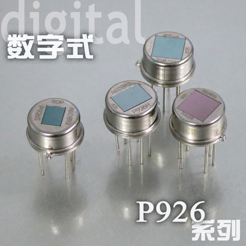
Features:
Using digital signal processing technology to process the pyroelectric signal.
A high impedance differential input as the sensing element input.
Uses a 16 bit precision AD converter to convert the voltage signal generated by the sensitive element into digital signal
Uses a two order Butterworth filter, to filter the digital signal, effectively filter various sources low frequency and high frequency noise.
Due to signal processing is completed in the shell shield,has the stronger ability of anti RF interference.
Threshold of sensitivity, ONtime can be adjusted by an external voltage.
With light sensor application input,sensors can be controlled to function below the set illuminance
Low power consumption
Detailed Description:
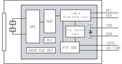
Schematic Circuit:
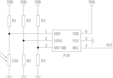
Alarm Event Processor
The signal from the band pass filter is rectified. When the signal level exceeds the set sensitivity threshold, an internal pulse is generated. A second pulse is counted, when the signals changes sign and exceeds the threshold again.
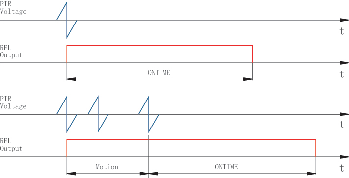
Whenever 2 pulses appear within 4s, an alarm condition is detected and the REL output is activated. If the signal level is in excess of 5 times the selected threshold, 1 pulse will cause activation of the REL output.
Sensitivity / Threshold
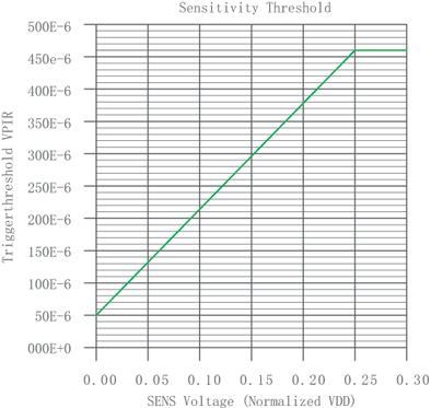
The voltage applied to the SENS input defines the threshold for the PIR signal which generates a pulse for the pulse counter, to determine an alarm condition. Connecting this input to VSS will result in the minimum possible threshold level, which is hardwired internally (offset) to avoid false detection due to zero threshold and detector noise. Any voltage above VDD/4 will select the maximum threshold, which is the least sensitive setting for PIR signal detection.
Hysteresis on the OEN input

ON TIME
The voltage applied to the ONTIME input determines how long the REL output stays active after the last alarm condition has been detected. If multiple alarm conditions are detected during the on time period, the on time is re-started whenever an alarm condition is detected. The on time period is derived from the oscillator frequency and will have a spread accordingly.
|
Step
|
Pin
voltage
Center
of step voltage value
|
ONTIME(s)
|
|
|
|
(VDD*(Step*2)+3)/128
|
(typ)
|
|
|
0
|
3/128 or
less
|
2.3
|
|
|
1
|
(VDD*2+3)/128
|
4.7
|
|
|
2
|
(VDD*4+3)/128
|
7
|
|
|
3
|
(VDD*6+3)/128
|
9.4
|
|
|
4
|
(VDD*8+3)/128
|
18.7
|
|
|
5
|
(VDD*10+3)/128
|
37
|
|
|
6
|
(VDD*12+3)/128
|
56
|
|
|
7
|
(VDD*14+3)/128
|
75
|
|
|
8
|
(VDD*16+3)/128
|
150
|
|
|
9
|
(VDD*18+3)/128
|
300
|
|
|
10
|
(VDD*20+3)/128
|
449
|
|
|
11
|
(VDD*22+3)/128
|
599
|
|
|
12
|
(VDD*24+3)/128
|
1198
|
|
|
13
|
(VDD*26+3)/128
|
2397
|
|
|
14
|
(VDD*28+3)/128
|
3595
|
|
|
15
|
(VDD*30+3)/128
or above
|
4793
|
|
